


 Toadenka Co., Ltd.

Most recent update: 2023-11-30
PR message
Toadenka K.K. is a research and development business which provides micro-level surface processing and nano-level functional thin film processing aimed at semiconductors, electronic devices, optical equipment, next generation automobiles, and other fields.
We contribute to the resolution of issues in fields which require ultra-high precision, ultrafine and ultramicro capabilities by pursuing unique technologies such as the mold release thin film TIER coat, developed through active research into triazine thiol compounds in industry-academia-government collaborations, and the TRI System which can bond metal and resins into a single piece using nano thin films.
<<Plating and special surface processing>>
●Various types of plating
Various plating processes including gold, copper, palladium/nickel, tin, solder, bright nickel, black nickel, chrome, zinc, electroless nickel (lead free), CPF lubricated nickel
Negotiable: Palladium
●Various types of chemical conversion processing
Chemical conversion processing of magnesium alloys (TOA-MG-1A)
Anode oxidization of aluminum and its alloys (alumite)
Trivalent chrome processing of aluminum alloys (alodine)
Stainless chemical conversion processing, etc.
●Functional thin film processing
Mold release thin film TIER coat
TRI System single piece bonding technology for metal and resins using nano thin films
TOANIC direct bridging adhesive technology for metal and high polymer materials
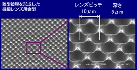
TIER Coat is a mold release film developed by Toadenka for plastic molding metal molds. It allows for molding of highly adhesive resins, such as clear epoxy resin, without using mold release agents by forming a fluorine nano scale film through vacuum deposition. It also displays superior release performance for silicon resins, urethane resins, and other adhesive resins.
<<TIER Coat Applicable Fields>>
Because the product is a thin film with film thickness of approximately 30 nm, it causes no damage to even microscopic shapes as in processing involving metal molds for microlens formation. It is expected to use in cutting edge fields, such as, in metal molds for mobile phone and handheld game optical films and metal molds for optical discs and microlenses.
<<TIER Coat Major Characteristics>>
The film has high durability due to strong adhesion through chemical bonding and has a proven track record in over 150,000 shots for thermoplastic resin molding.
Possessing a thin, film thickness of 30 nm, allows for drastic improvements in production efficiency and product yields compared to older methods involving application of mold release agents for each molding process.
It also possesses superior water repellent properties, making it effective at preventing stain as well. Since recoating is possible, the product also allow for molds to be reused.
<<TIER Coat Physical Properties, etc.>>
1. Film thickness: Approx. 30 nm
2. Contact angle: Ethanol 55-60°
3. Solvent resistance: There was no decrease in release performance after immersion testing in the following solvents.
n-hexane, cyclohexane, isopropyl alcohol, ethanol,
xylene, diethyl ether, tetrahydrofuran,
acetone (Testing conditions: Immersed for 360 hours at room temperature)
4. Metal mold materials on which film formation is possible:
Iron materials, stainless materials, chrome plating, electroless nickel plating
Electrical nickel plating (electroformed nickel)
5. Mold temperature at time of molding: -250ºC
*TIER Coat is an organic film so it will be damaged if rubbed with hard items (metal, glass filler, etc.), losing its effectiveness.

The TRI System is a single piece bonding technology for metal and resins which utilizes Toadenka's original nano thin film technologies.
This technology allows for metal and resins to be bonded into a single piece without adhesives by using a technology where a bonding film with high chemical reactivity to both metal and resins is formed in addition to insert molding technology.
In normal insert molding, it is necessary to process the shape of the metal which will serve as the bonding mechanism. In addition, the process also resulted in gaps in the bonded surfaces, making for poor seals.
In this technology, even bond is formed by manifesting the bonding mechanism on to the metal surface (chemical bonding) and a firm. This means there is no need to machine the bonding surfaces and allows for free design of the part shapes. In addition, this creates a bonding strength superior to that of adhesive intermolecular force bonding, which provides superior seals, pressure resistant water proofing, oil proofing and heat resistance.
These outstanding qualities allow for the technology to be used in vehicle mounted with lithium ion rechargeable battery seal port plate seals and it has been proven in use in HONDA FCX fuel cell automobile ultra-capacitor parts.
[Metals and resins which can be bonded]
・Metallic copper, aluminum, other
・Resin PPS, PBT, other
Recipient of the "Aoki Technical Laboratory" Technology Award

A new wet plating method for plastic materials.
A new process where etching (surface roughening) is miniaturized to a nano level of approximately 15-50 nm and then used as an anchor for the plating, which allows for addition of functionality, such as, metallization of the entire surface without losing the materials surface conditions or fine shapes and complex shapes.
For resin screws like those in the photo, thin film plating electroless Ni onto the nano-etched anchors adds a metallic exterior without affecting the concave and convex shapes.
In addition, by finishing the product to thickness of 0.1-0.3 μm, required in order to achieve a glossy appearance of the plating film thickness after nano-etching, it can be used for a wide variety of applications and fields including "adding a metallic exterior to mirror finished resin materials" and "hologram-like diffraction grating processing".
<<Nano-etching plating compatible materials>>
・Polycarbonate
・ABS
・Polycarbonate/ABS alloys
・Polyurethane
・Acrylic (Limited to hard coat products)
・Acrylic ultraviolet curing resins
*Contact us for information on resin materials other than the above.

TOA-CPF (lubrication coating) is a film with PTFE (resin particles of 1 micron or less) mixed in electroless nickel platting film in order to provide lubrication.
This is used, for example, in printer shafts and PC FD, CDD and DVD drive parts. In addition, the unique black coloration is a Toa original feature. The beautiful hue grabs attention.

Circuit / electrode plating technology plays an important role in surface processing which serves as one of the important technologies for Molded Interconnect Devices (MID). MID is a technology which allows for flexible formation of circuits and electrodes on resin molded products.
Designing and manufacturing of unified mechanisms and circuits allow for part miniaturization and weight reduction.
(Recipient of the "Aoki Technical Laboratory" Technology Award.)

Corrosion resistance, conductivity, and painting film adhesion are required for magnesium alloy chemical processing, so it is necessary to form a chemical conversion film in advance.
Toadenka is able to produce these required characteristics through the formation of the unique thin chemical films of 0.1 microns or less developed by our company.
The environmentally friendly non-chrome films are used to achieve lighter weight casings for mobile phones, digital cameras, PCs, and other products.

At Toadenka, we are able to metalize adhesion of materials through chemical bonding between metals and high polymer materials (rubber, resin, paints, etc.) that previously would have been impossible through usual nano level film forming technologies based on functional films created through active research of triazine thiol compounds.
Chemical bonding between a metallic surface and a high polymer material (rubber, resinous, paint, etc) occurs simultaneously as high polymer materials are bridged (become high polymer materials).
Various types of materials including liquids, films, thermoset chemicals, and ultraviolet curing chemicals, can be bonded. The thickness of the thin film between the metal and high polymer materials is only from 10 to several 100 nm. This means the process is not limited by dimensions or shapes.
The entire semiconductor lead is processed for soldering.
(Lead free tin bismuth plating, pure tin plating, etc.)
Toadenka uses advanced processing technologies to handle semiconductor materials, which come in a variety of forms, and provides consistent service including strict quality management.

| Company name | Toadenka Co., Ltd. | Website URL | http://www.toadenka.com/ |
|---|---|---|---|
| Street address |
Morioka-shi Gyokusan-ku Sibutamizi iwahana Iwate Japan
[See map] |
Person in charge | Shuhei Miura |
| Telephone number | +81-19-683-2101 | Fax number | +81-19-683-1337 |
| Capital | 35,000,000 JPY | Employees | 115 |
| Annual sales | 1,040,000,000 JPY | EMIDAS Member Number | 88923 |
| Type of manufacturing | Industrial machinery / Electronic parts / Electrical component for transportation equipment | ||
| Main 3 products |
|
||
| Large | Medium | Small |
|---|---|---|
| Surface treatment | Plating/Chemical conversion treatment | Zinc (barrel) Nickel (rack) Tin (rack) Copper (rack) Chromium (rack) Alumite (anode oxidation) Aldine treatment (aluminum chromate) Electroless nickel (rack) Chemical conversion coating Iron Copper Brass Zinc die-cast Aluminum Stainless steel Plastic Magnesium Hard alumite Black nickel |
| Surface treatment | Polishing/Lapping | Chemical polishing |
| Surface treatment | Barrel polishing | Barrel finishing (vibration) |
| Surface treatment | Other surface treatment | Vacuum deposition |
![]()