- Telephone number: +81-22-777-1351
- FAX: +81-22-777-1357
- Website
- Basic Info
- Equipment
- Technology & Products
- History, Philosophy & Quality
- Map / HQ
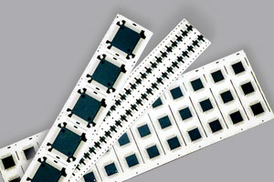
Environmental Regulatory Compliant Lead-Frame Outer Layer Plating
Industry
Semiconductor
Specifications
- Materials:Iron
- Lots: ---
- Precision:1/1,000 mm or less
Conventional technologies/differences from other companies
Environmental Regulatory Compliant Lead-Frame Outer Layer Plating
◆Characteristics
In order to comply with RoHS and other environmental restrictions, and to use as an alternative of IC Lead-frame Sn-Pb solder outer plating, we can mass-produce products with Sn plating/Sn-Bi plating.
・High reliability and achievements since 1982 on lead frame outer layer plating.
・Can analyze amount of RoHS restricted substance amount using ICP emission spectrophotometric analyzers.
・reduced process by in-line deflash (removing mold resin within the line).
・Just-in-time manufacturing with 365 days, 24 hours.
・Guarantee quality with SPC (Statistical Process Control)
Please contact us for details of plating evaluation results.
◆Uses
Semiconductor lead frames: 42 alloy (steel – nickel alloy), copper alloy.
Company info
| Company name | KEDICA CO.,LTD. | EMIDAS Member Number | 49256 |
|---|---|---|---|
| Country | Japan | Street address |
Sendai Izumi Miyagi Japan |
| Telephone number | +81-22-777-1351 | Fax number | +81-22-777-1357 |
| Employees | 98,000,000 JPY | Annual sales | |
| Employees | 151 | Person in charge | Atsushi Uchimi |
| Type of manufacturing | Industrial machinery / Telecommunication equipment / Electronic parts | ||
| Primary clients |
|
||


