Mitsuya Co., Ltd.

Most recent update: 2026-08-07
PR message
Discover Next-Gen Surface Treatments with 90+ Years of Expertise!
Backed by over nine decades of innovation, we offer 100+ advanced surface treatment technologies engineered to meet your toughest manufacturing challenges.
What we bring to the table:
• Ultra-High-Precision Plating: Perfect for probe pins and micro-components.
• Precious Metal Solutions: Superior conductivity, durability, and corrosion resistance.
• Hard-to-Plate Materials: Seamless adhesion for complex substrates.
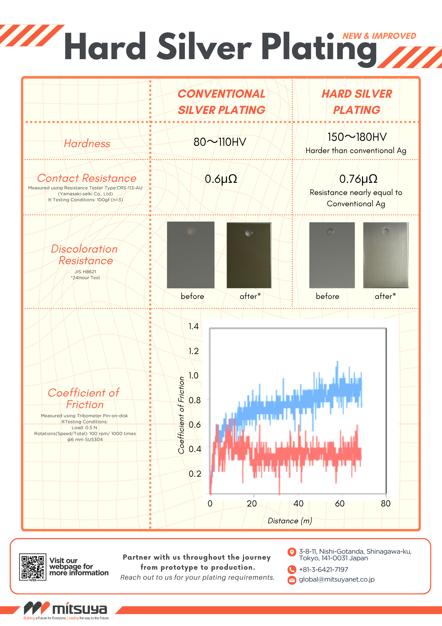
Standard silver plating (80–110 HV) is prized for high electrical conductivity, but its soft nature makes it highly susceptible to mechanical wear, high friction, and surface tarnishing/discoloration over time. In high-cycle sliding contacts and high-power connectors, conventional silver coatings wear down rapidly, causing contact failure and requiring frequent component replacement. Moreover, attempts to harden silver coatings often severely compromise conductivity or contact performance.
Our Competitive Advantages & Key Differentiators:
Mitsuya’s new & improved Hard Silver Plating achieves significantly higher hardness (150–180 HV) while maintaining low contact resistance (0.76 µΩ, nearly equal to conventional silver’s 0.6 µΩ).
・Superior Mechanical Hardness & Low Friction: Delivers 150–180 HV hardness and a substantially lower coefficient of friction compared to conventional silver, dramatically reducing wear during repeated insertion and sliding cycles.
・Enhanced Discoloration Resistance: Formulated to resist surface oxidation and discoloration (tested under JIS H8521 24-hour testing), ensuring long-term visual and electrical stability.
・Applicable Substrate Materials: Suitable for direct plating onto Copper, Copper Alloys (Brass, Phosphor Bronze), Stainless Steel (SUS), Aluminum, and Nickel/Steel Substrates.
・Target Industries & Key Applications: Ideal for Automotive & EV (high-voltage connectors, charging plugs), Semiconductors & Electronics (switches, high-cycle testing probes), Power & Energy (heavy-duty switches, busbars), and Industrial Equipment (sliding contacts and high-wear components).
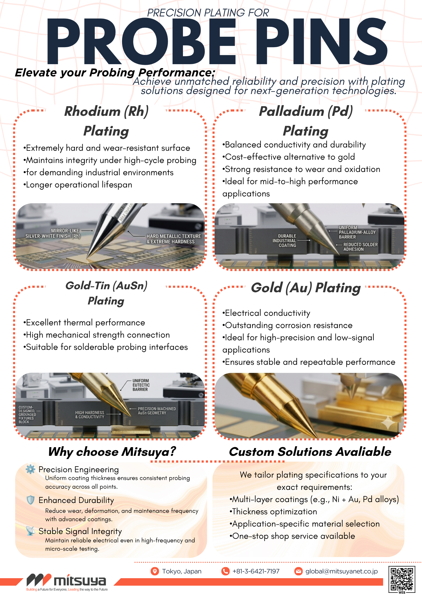
Probe pins used in semiconductor inspection and micro-scale testing face extreme operational demands, including millions of contact cycles, high frequencies, and exposure to oxidation. Conventional plating techniques struggle to balance contact resistance, mechanical hardness, and uniform thickness across ultra-fine pin geometries. Poor plating consistency leads to unstable signal transmission, premature contact tip wear, pin deformation, and frequent equipment downtime during high-throughput semiconductor testing.
Our Competitive Advantages & Key Differentiators:
・Mitsuya provides ultra-high-precision plating solutions tailored specifically for next-generation probe pin applications, delivering unmatched signal reliability, wear resistance, and operational lifespan.
・Diverse Precious Metal Coatings: We offer specialized deposits matched to your exact testing environment:
・Rhodium (Rh): Extremely hard surface for extreme wear resistance and extended pin operational lifespan in high-cycle testing.
・Palladium (Pd): Balanced conductivity and wear/oxidation resistance as a cost-effective alternative to gold.
・Gold-Tin (AuSn): Exceptional thermal performance and high mechanical strength for solderable probing interfaces.
・Gold (Au): High electrical conductivity and corrosion resistance for low-signal, high-precision applications.
・Precision Engineering & Uniformity: Micro-thickness controls guarantee consistent coating thickness across complex pin geometries, maintaining stable electrical contact even in high-frequency and micro-scale testing.
・Fully Customizable Multi-Layer Solutions: We provide bespoke plating configurations (e.g., Ni + Au, Pd alloy underlayers), thickness optimizations, and application-specific material selection through a seamless one-stop process.
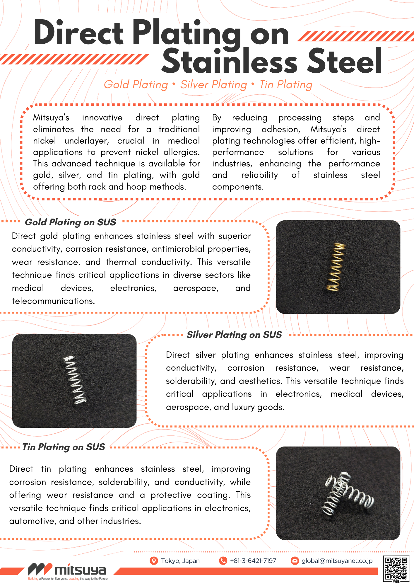
Traditionally, plating on stainless steel (SUS) requires an intermediate nickel underlayer to ensure proper adhesion. However, nickel poses significant risks of skin irritation and metal allergies, making it unsuitable for medical, wearable, and high-precision applications. Furthermore, attempting direct plating without an underlayer usually leads to poor adhesion and peeling due to the passive oxide film on stainless steel substrates.
Our Competitive Advantages & Key Differentiators:
・Mitsuya’s proprietary direct plating technology completely eliminates the need for a nickel underlayer, enabling direct gold, silver, and tin plating directly onto stainless steel components.
・100% Nickel-Free Safety: Ideal for medical devices, wearable electronics, and luxury goods where allergy-free safety and high biocompatibility are essential.
・Streamlined Process & Cost Reduction: Skipping intermediate underlayer steps shortens manufacturing lead times, reduces processing costs, and improves overall yield.
・Superior Adhesion & High Functionality: Our specialized pre-treatment overcomes passive oxide layers to achieve exceptional direct adhesion, ensuring maximum conductivity, corrosion resistance, and wear durability.
・Flexible Processing Methods: We offer flexible processing solutions, including both rack and hoop (reel-to-reel) methods, tailored for micro-springs, complex components, and continuous materials.
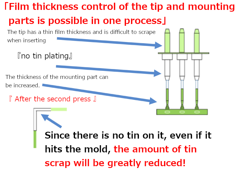
Tin plating is widely used in electronic components due to its excellent solderability. However, conventional tin plating is highly prone to "tin whiskers"—microscopic, needle-like crystals that grow on the plated surface and cause critical electrical short circuits. Furthermore, modern terminal designs increasingly demand dual functionality (e.g., both press-fit areas and soldering areas) on a single component. Traditional uniform-thickness plating methods struggle to fulfill these dual requirements without causing manufacturing issues, such as tin debris clogging dies during post-bending processes.
Our Competitive Advantages & Key Differentiators:
・Mitsuya resolves these challenges by integrating advanced thermal reflow treatment with highly customizable differential plating techniques.
・Whisker Growth Suppression: By applying a post-plating reflow treatment, we melt and recrystallize the tin layer, effectively preventing tin whisker formation and significantly increasing component reliability in critical electronics.
・Differential Thickness Plating for Dual-Purpose Terminals: We can precisely vary plating thickness across the same terminal—applying a thin tin layer (e.g., 0.5 µm) to the press-fit section and a thicker layer (e.g., 2.0 µm) to the soldering area.
・Tooling Protection via Selective Layer Exposure: To prevent tin buildup on stamping dies during post-forming or bending operations, we can selectively expose the underlying nickel plating in specific bend areas, ensuring smooth manufacturing and long tool life.
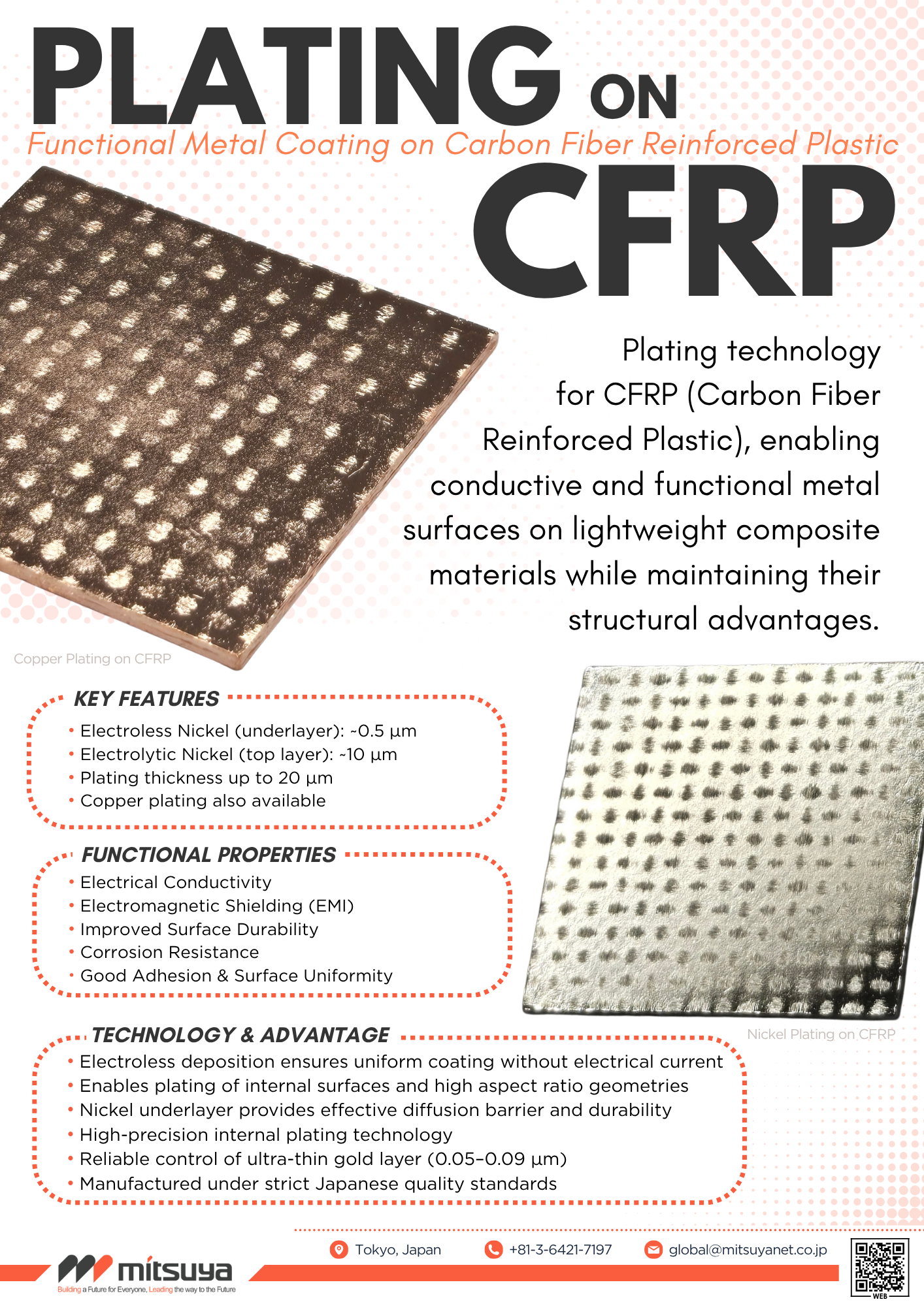
While Carbon Fiber Reinforced Plastic (CFRP) is widely recognized for its ultra-lightweight and high-strength structural advantages, applying functional metallic coatings onto carbon composite substrates is notoriously difficult. Conventional surface treatments often suffer from poor adhesion, uneven coating thickness across complex or high-aspect-ratio geometries, and limited functional capabilities—frequently compromising the material's underlying structural benefits or failing to deliver sufficient electrical conductivity and shielding.
Our Competitive Advantages & Key Differentiators:
・Mitsuya’s specialized CFRP plating technology imparts metallic surface functionality—such as electrical conductivity, EMI shielding, and enhanced durability—onto lightweight composite materials without sacrificing their core structural advantages.
・Advanced Multi-Layer Coating Options: We offer tailored coating stacks, including electroless nickel underlayers (~0.5 µm), electrolytic nickel top layers (~10 µm), total plating thicknesses up to 20 µm, as well as copper plating and reliable ultra-thin gold layer control (0.05–0.09 µm).
・High-Precision Complex Geometry Plating: Electroless deposition ensures completely uniform coverage without electrical current, allowing precise plating on internal surfaces, high-aspect-ratio geometries, and intricate composite parts.
・Superior Functional Performance: Delivers exceptional electrical conductivity, electromagnetic interference (EMI) shielding, surface durability, corrosion resistance, and robust metal-to-substrate adhesion.
・Strict Quality Control: Processed and manufactured under rigorous Japanese quality standards to ensure high reliability for aerospace, automotive, and high-tech industrial applications.

 |
Aluminum( Surface treatment / Plating/Chemical conversion treatment ) |
|---|


| Company name | Mitsuya Co., Ltd. | Website URL | https://www.mitsuya-plating.com/ |
|---|---|---|---|
| Street address |
Shinagawa-ku Tokyo Japan
[See map] |
Person in charge | ohsuga |
| Telephone number | +81-3-3492-7197 | Fax number | Log in to display |
| Capital | 15,000,000 JPY | Employees | 298 |
| Annual sales | Unregister | EMIDAS Member Number | 63028 |
| Type of manufacturing | Telecommunication equipment / Electronic parts / Electrical component for transportation equipment | ||
| Main 3 products |
|
||
| Large | Medium | Small |
|---|---|---|
| Surface treatment | Plating/Chemical conversion treatment | Nickel (barrel) Copper (barrel) Chromate (general) Nickel (rack) Tin (rack) Copper (rack) Gold/Silver plating Zinc (rack) Alumite (anode oxidation) Acid pickling Aldine treatment (aluminum chromate) Electroless nickel (barrel) Electroless nickel (rack) Baking (hydrogen embrittling) Copper Zinc die-cast Aluminum Stainless steel Black chromate (black/green) Colored chromate (multi-color) |